Tuesday, January 30, 2024

Recapping Caps0ff

 (repost from Patreon)

To recap on the project's history, Caps0ff entered the scene some years after the incumbent arcade decapper was no longer available. We were able to triage the chip stash with fresh eyes and  get things moving again.

Unfortunately, as is likely evident, this project has been on hold for quite a while, both in terms of pausing pledges as well as work put into it. However normally during the holidays I'm at least able to catch up a bit and put some time into making at least some progress. However, as my life has evolved the holidays were instead spent on catching up on normal life.

Additionally, while there was always one primary contributor, the team includes a number of critical support roles (PCB design, ROM decoding, etc). While some of these team members are still available, it creates additional friction to coordinate restarting the pipeline.

With all of this in mind I don't see a regular cadence resuming in the near future. While the project will continue ad-hoc as possible I don't believe its in anyone's best interest to maintain this Patreon. Namely it is unnecessary distraction / pressure for me to keep remembering to pause it and, if forgotten, its not appropriate to charge people for work not done. This can cause both sides to get frustrated.

So what do I see as the next steps? First, the chips will remain here until either I can put more work into it or find a new champion. Unfortunately the previous attempt to farm out some chips did not work out, so this will require some thought how to do this appropriately. That aside, there are now many more "chip decappers" out there when this project started. So I'm optimistic that someone will be interested and qualified to pick up the torch. And I'm happy to work with them to pass off general knowledge and pedigree on the chips. In lieu of directing funds my way, please join their Patreons and help them on their journey. I will leave this notice up for a bit and then formally shut down this account.

I sincerely thank you all for supporting this project. Its quite expensive to run and Patreon really helped to keep things moving. Stealing a quote from a friend: "May all your die shots be clean, your laser hits on-target, and your glitches fast enough in 2024!"

Thursday, February 25, 2021

February laser glitching w/ P87C52EBPN and more

In this post we give some brief status updates on recently completed and in progress projects. The main focus is using a laser to glitch security circuitry on several 8051 based MCUs from vintage arcade cabinets. Preserving this firmware allows people to better understand these games as well as fix broken cabinets.


Recently we preserved the firmware from a few MCS51 chips via laser glitching. First, Cookie & Bibi 2 is a tile matching puzzle game from Taito. It's based on Puzzle Bobble which is in turn based on Bubble Bobble.


In particular we are taking a look at preserving the firmware of the P87C52EBPN at lower left:


We've processed a few P87C52EBPN before and were surprised to find several very distinct chips all marked "P87C52EBPN." It's unclear if these were remarked or we just didn't understand Phillip's package marking scheme. In any case, here is the new die:


Above: new die (Cookie & Bibi 2 P87C52EBPN as XSC6407A)

Which is close to one we already saw:


Above: previous P87C52EBPN as XSC6644A

Note the lighting is different on these two die shots (metallurgical vs inspection microscope) but the overall layout is very similar. Still this is unfortunate because we didn't have any sample chips to test an attack against. However:

  1. We've been able to develop attacks against similar chips fairly reliably
  2. A replacement chip (board) would be about $60

Given this we decided to try to develop the attack on the actual target without practicing first. We found the structure used in the previous article and found shining a laser on it gave a stable read out! We probed around a little more though and got a second binary that was also stable. There should only be one correct binary coming out. So how did we get two distinct binaries?

Often we run binaries through checker scripts that look for common errors like stuck address or data lines. When we ran these two binaries through they flagged some issues:

  • Binary 1 has bits 7 and 8 stuck high
  • Binary 2 has bit 8 stuck high

So actually neither is correct, but might be close. We then integrated the binary checker into the fuzzing script to get quicker feedback. After a bit more searching we locked onto a location that passed all checks and also saw some strings:


Now with all bits toggling and strings visible we have a plausible dump! One early concern was a relatively unusual reset vector, but analysis shows it's fine.

We also did a small project with S87C751 from World Beach Volley:

Above: "MAIN" board w/ chip. Handles sound

Above: "LINK" board (chip was at right). Handles extended multiplayer

One chip is marked "MAIN" and the other is marked "LINK." The smaller link board adds two additional players allowing up to four people to play at once.


After a bit of poking around we found a glitch as seen above. The layout seems to loosely resemble what we saw on P87C52EBPN and is probably the same basic glitch on both chips.

Currently we are looking at a few programmable logic chips such as PAL16R8A2NC. This chip can be extracted a number of ways including electrically testing all input combinations, imaging burned fuses, or microprobing. We have several of these methods under evaluation and it will hopefully be the subject of our next post. Finally, this project has pushed back some more conventional mask ROM captures that are queued such as Apple ADB PICs.

Enjoy this post? Please support us on Patreon or follow us on TwitterNote: with the Indiegogo campaign over we unfortunately don't currently have a way to accept one time donations.w

Tuesday, December 1, 2020

If at first you don't succeed boil it in acid


In a previous post we discussed extracting TMS32010 ROMs optically. This information helps the arcade community better understand these cabinets for repairs and historical reference. In this post we investigate later generation TMS320 using a combination of electrical test interfaces and microscope images.

The first generation Digital Signal Processor (DSP) chips in the first post were succeeded by the TMS320C10 and then the TMS320C25 as seen above. This is Namco Winning Run's TMS320C25FNL (decap G82) which was extracted via a similar decapping and imaging process as TMS32010. It's part of Namco System 21 where it accelerates 3D graphics operations. Additional analysis will give the community a much deeper understanding of how the graphics engine works. Special thanks to Nathan Gilbert for converting microscope images into firmware!

TMS320C25 was then succeeded by TMS320C5X which is the focus of this article.


The origin of the TMS320C5X project is a TMS320BC53PQ80 found on Taito Operation Tiger. Similar to the Winning Run TMS320, Operation Tiger uses TMS320 as part of it's graphics engine and detailed analysis will help the community understand how it works. This was thought to possibly be a straightforward project as these chips have several digital interfaces that might be used to quickly extract firmware.


To make things easy we got a TMS320C5X DSP Starter Kit (DSK) development board with matching software. It has a very similar part (TMS320C50 vs TMS320BC53) in the same footprint which should allow us to run some tests and then transplant the target chip onto the DSK board.

This is roughly our understanding of how the intended development flow works:

  • Tiny mask ROM firmware loads an external PROM
  • External PROM knows how to talk to serial port
  • DOS system downloads debug kernel over serial port
  • Debug kernel can load additional programs
We can omit the last step since we just need to send simple commands to the debug kernel. Let's see if we can get that running.

The big catch is that the software runs on DOS with unusual serial port settings (ex: 2 stop bits) which caused some setup issues. The DSK uses this to automatically detect baud rate based on timing between the first command data bits and the stop bits. In the end, VMWare with an FTDI adapter did the job.


Once the software is up it's relatively straightforward as there are commands to dump memory to files. The only catch is that they have a bug/feature where address 0 can't be saved, but can be seen in the visual display. So we save most of the data and then manually patched the word at address 0. And so we have the TMS320C50 bootloader!

Now to try the same thing but with TMS320BC53.

Source

However we weren't sure if this would work as the external PROM firmware was written for TMS320C50 which has a different address layout than TMS320C53.

We swapped the chips and unfortunately it's not working. We put a logic analyzer on and are able to show that DOS is communicating with the board but then something goes wrong. Specifically above shows PROM memory fetches changing in response to serial port data. We can possibly adjust the PROM firmware but there are a few more options to explore.

What about JTAG support? Even if this works we have a few chips that support JTAG but not the bootloader (ex: Winning Run). So seems like a good excuse to investigate that.

Unfortunately while these chips attempted to support JTAG there are several major issues. First, their JTAG implementation is non-compliant, making it incompatible with many adapters. Second, when it does work it's very bare bones and doesn't even support common instructions like IDCODE.

Most importantly though even with the right adapter the software is very difficult to setup. The only reference we could find involved patching a very specific version of Code Composer Studio version 3. And even then this probably only gave you TMS320C25 support which we'd then have to extrapolate to TMS30C50.

We tried to find some older DOS software that might support some form of XDS510 (such as the original ISA card above) but were unsuccessful. Since completing this project we have received additional software that might help if we encounter more TMS320. That said, if you have more TMS320 software, especially related to JTAG, we'd love to hear from you.

Anyway this means JTAG is not going to be easy. In the spirit of moving forward we begrudgingly decapped the chip and imaged the ROM.  While somewhat labor intensive this has a relatively straightforward path to completion.


Official designation is TMS320C53CS programmed with ROM D17336.


Zooming in on the ROM you can see it's very sparsely populated: there are a few bits at the top middle, and a few at the bottom. This makes sense as it only has a minimal bootloader and the vast majority of the code is in the external PROM.

A few puzzles though. First, why do the empty areas alternate 1's and 0's? Second, why is code split between the top and bottom? Fortunately we have the ROM from the TMS320C50 which significantly accelerates decoding. Take this section after the initial firmware:

00000270  be 4d bf b0 00 ff 6d 68  90 68 be 1f a7 68 b8 01  |.M....mh.h...h..|

00000280  be 1e 7b 90 01 31 69 66  be 20 be 4d e0 00 01 46  |..{..1if. .M...F|

00000290  be 4c ec 00 79 80 01 49  ff ff ff ff ff ff ff ff  |.L..y..I........|

000002a0  00 00 00 00 00 00 00 00  00 00 00 00 00 00 00 00  |................|

000002b0  00 00 00 00 00 00 00 00  00 00 00 00 00 00 00 00  |................|

000002c0  ff ff ff ff ff ff ff ff  ff ff ff ff ff ff ff ff  |................|

000002d0  ff ff ff ff ff ff ff ff  ff ff ff ff ff ff ff ff  |................|

000002e0  00 00 00 00 00 00 00 00  00 00 00 00 00 00 00 00  |................|

000002f0  00 00 00 00 00 00 00 00  00 00 00 00 00 00 00 00  |................|

00000300  ff ff ff ff ff ff ff ff  ff ff ff ff ff ff ff ff  |................|

00000310  ff ff ff ff ff ff ff ff  ff ff ff ff ff ff ff ff  |................|

We can see the transition from normal firmware to an alternating 1/0 fill pattern. While it's unclear why they do this, it's likely this is the actual ROM pattern as opposed to say obfuscation. Our best guess why they do this is that it plays a similar role to CMP fill on planarized ICs. That is, if it was filled with one polarity it would deviate a lot more from normal data and could cause yield issues. We couldn’t find an introductory article to link, but check out something like this for more information.

Anyway, also note our TMS320C50 dump has a footer:

00000f00  ff ff ff ff ff ff ff ff  ff ff ff ff ff ff ff ff  |................|

00000f10  ff ff ff ff ff ff ff ff  ff ff ff ff ff ff ff ff  |................|

00000f20  00 00 00 00 00 00 00 00  00 00 00 00 00 00 00 00  |................|

00000f30  00 00 00 00 00 00 00 00  00 00 bc 00 5d 07 00 30  |............]..0|

00000f40  ae 11 00 00 8b 8d bf 0d  80 00 bb 02 a5 a0 07 fd  |................|

00000f50  f4 00 5d 6a 80 00 5d 26  02 f0 5e 26 ff ef b9 f8  |..]j..]&..^&....|

00000f60  88 22 88 32 ae 21 a5 96  ae 31 59 a3 b4 01 be c5  |.".2.!...1Y.....|

Sometimes chip memory gets divided into pages to break up memory into small sections. It looks like TMS320C50 has one page and TMS320BC53 has four pages, so we think these might be page footers.

With this in mind Nathan Gilbert did the heavy lifting here. First he decoded the four pages separately and munged until they roughly resembled the TMS320C50 data. We then compared footers between pages and found bits to order the pages as labeled above. These bits are believed to be an absolute address as part of an assembly routine but significant analysis has not been done.

Now with the ROM decoded we can compare TMS320C50 and TMS320BC53. While the main firmware is identical the footer has a number of differences. We don't believe anyone has yet looked into specifics.


Finally, there was a brief effort to decode an unknown TMS320C52 wafer with a large amount of firmware. Someone attempted to use computer vision to automatically extract the bits but it was ultimately abandoned due to some combination of insufficient data quality and low perceived impact of having a successful decode.

That about wraps it up. Lots of people helped complete this project! Special thanks to the following:

  • Nathan Gilbert: decoding, bit typing
  • jordigahan: board purchase
  • ClawGrip: board purchase
  • Montornés Solé: board purchase
  • Philip Åkesson: bit typing
  • James Sun: bit typing

Enjoy this post? Please support us on Patreon or follow us on TwitterNote: with the Indiegogo campaign over we unfortunately don't currently have a way to accept one time donations.

Wednesday, November 4, 2020

Extracting the elusive TMS32010 mask ROM

In the late 1970s Texas Instruments made the TMS5100 for the Speak and Spell. This special purpose processor could quickly do math operations required for speech synthesis. This is an early form of Digital Signal Processing (DSP) where code creates signal digital filters instead of using discrete components like capacitors and resistors. Following the success of that project they looked into higher performance DSP architectures which resulted in the TMS320 family being released in the early 1980s.

This was welcome news to game designers of the 1980s. Arcade machines require a wide variety of high performance audio and video processing. Unfortunately CPUs of the day were relatively slow meaning  cutting edge games required expensive custom logic made with large circuit boards or custom ASICs. DSPs introduced a new option by focusing on high performance math operations rather than traditional code execution.

Specifically the first generation TMS320 included the TMS320M10, a version with 3K bytes of mask ROM. This was used in a few Toaplan games like Flying Shark (decap G72, G210) and Kyukyoku Tiger (also known as Twin Cobra, decap G71):

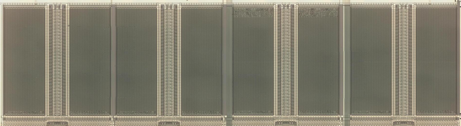
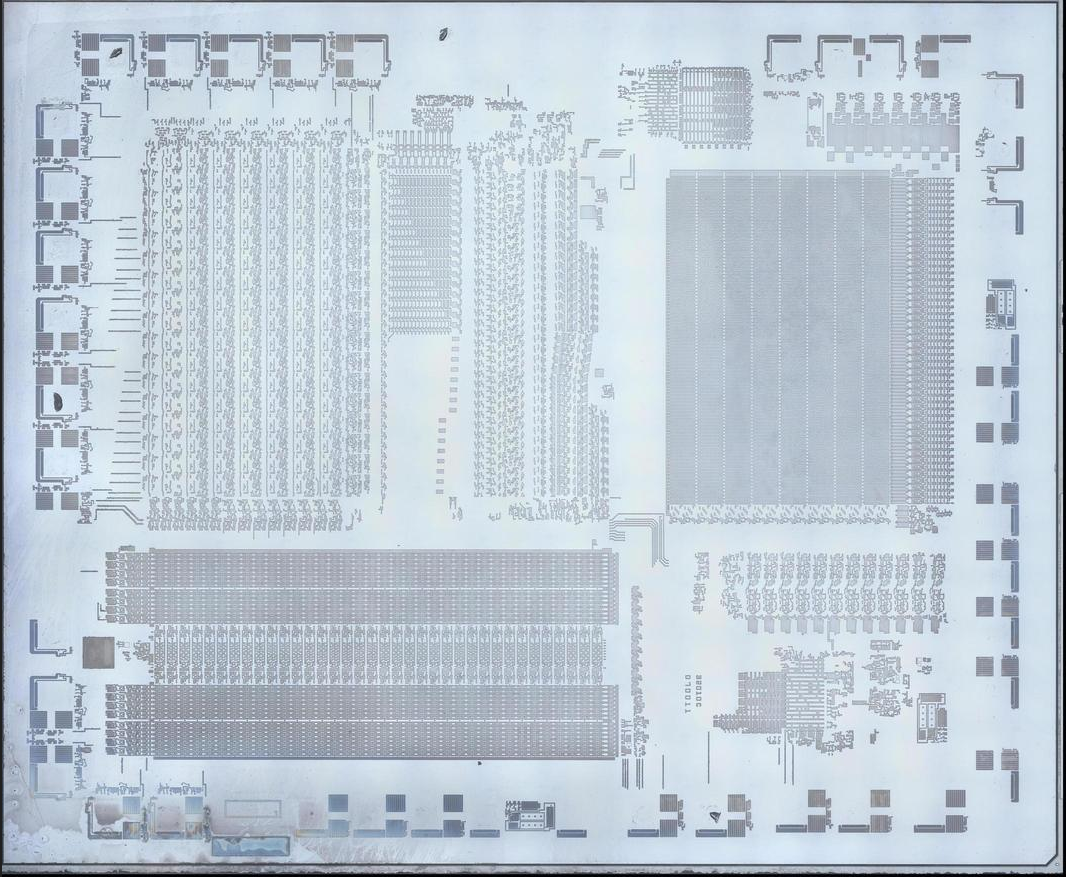
More info can be found here. Anyway, here's a TMS320M10 die shot:

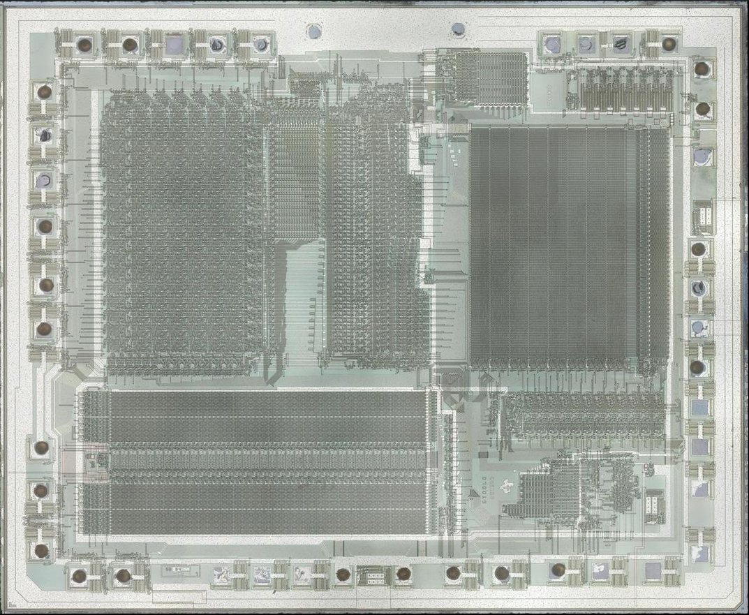
Close up of the logo:


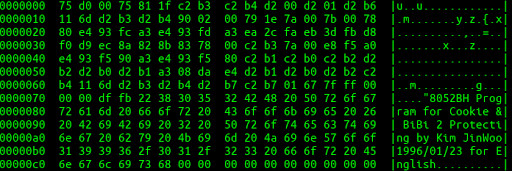
Note the die part number is "32010C", not "320M10" as in marketing material. This is similar to how "TMS5100" is a marketing name but its internally a "TMC0280." Also note the second line of text, diffusion on the silicon substrate, matches the package:


Checking out the ROM area we vaguely see bits but with poor contrast:


Zooming in helps a little, but its still pretty hard to read:


Looks like it might be a diffusion ROM and delayering to silicon substrate will improve contrast. This is consistent with D70015, presumably the mask ROM ID, being encoded in diffusion. Die after delayering:

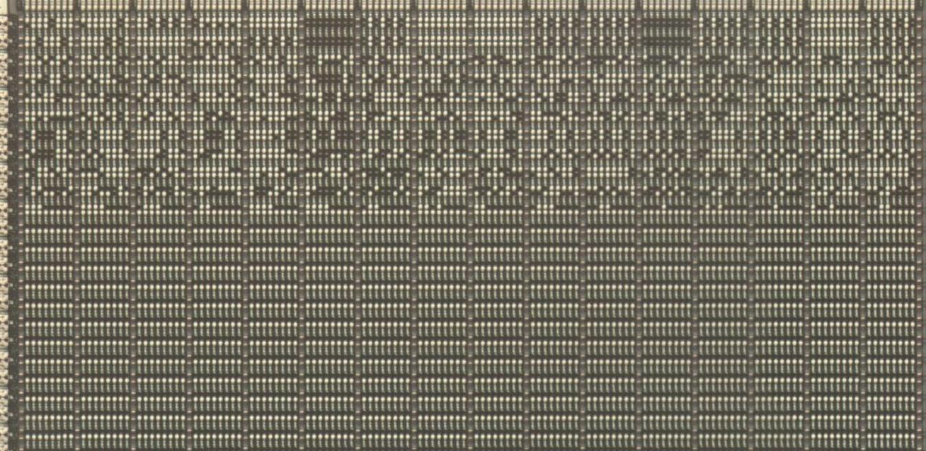
The ROM is now way easier to read:

Now we can also see the contrast issue: the polysilicon and metal was mostly overlaid on the diffusion lines above, hiding most of the detail. Now that the polysilicon and metal is removed the bits can be resolved clearly.

Next the ROM photograph is converted into a 2D bit array so we can figure out the bit order. Usually bit order is very linear, such as grouping bits into columns with the least significant bit at the left and most significant bit at the right. Consider a 4 bit CPU with this ROM layout:

Where:

  • B0 means bit 0, the least significant bit and B3 is the most significant bit
  • Bits are grouped into columns
  • Each bit column starts upper left, scans right, and then wraps around to the next row

Lets say your ROM is typed as:

01 10 10 10
00 10 01 11
Where spaces have been added to emphasize the bit columns and the first word is highlighted in bold. Using the decoding scheme above results in the following 4 bit words:
  • 0xE
  • 0x1
  • 0xA
  • 0xC
Unfortunately there are many variants on this type of scheme and it may not be obvious which scheme is used in this particular type of memory. However  there are a couple of ways to narrow it down:
  • Reverse engineer logic and deduce the scheme from first principles
  • Make educated guesses
The first always works, but can be a lot of effort. Instead, we usually rely on the fact that most architectures have a few regular patterns that we can look for. For example, here are a few TMS32010 binaries disassembled:

000: f900 0010  b    0010h
002: f900 00af  b    00AFh
...
010: 7f8a       rovm
011: f500 0013  bv   0013h

000: f900 0004  b    0004h
002: f900 0d96  b    0D96h
004: 7f81       dint
005: 7f8a       rovm

000: f900 00d7  b    00D7h
002: f900 0642  b    0642h
...
0d7: 7f8b       sovm
0d8: 6e00       ldpk 0
It looks like a pretty good guess for the first word and third word is 0xF900. Let's use this as a heuristic to determine if we have the correct memory layout.

It's also worth mentioning we don't yet know the bit polarity: does a squiggle in the image mean it's a 0 or a 1? One way to intuitively deal with this is to think about things more in terms of bit transitions or hamming distance than the actual values. If using a program to extract the bits we usually try both polarities and see which works better.

Unfortunately we tried a few simple layouts and didn't see 0xF900's coming out. Fortunately Nathan Gilbert volunteered to help and had several major contributions. First, he digitized all three ROM photographs into bits in a .txt file. The bits are then compared between chips which shows where common data is. In particular this gives us a hint which side of the memory layout the initial branch instruction, 0xF900, might be.

Nathan then poured over the bits in great detail but had trouble finding a simple solution. Next he looked at our die shots to see if they provide hints. For example, they show how large memory blocks are and may show things like unusual bit ordering on data buses.

Unfortunately we were still struggling. But we thought we might have a silver bullet: a previous project had decoded the BSMT2000 audio chip, a TMS320C15. Maybe we could dig up this data, study the encoding, and use that to decipher the order?

We found the binary and bsmt2000 scanning electron microscope (SEM) images from Dr Decap:


Unfortunately we didn't find any info on the bit ordering or the intermediate photograph typed bits, but having the final binary and the source image is a good starting point nonetheless.

Zooming in on some bits:


Where bits are represented by contacts shown in bright white. But that's a problem: TMS32010C is a diffusion ROM while TMS320C15 is a contact ROM. This means it may not help decoding TMS32010C. 

First, you can figure out high level structure without knowing the exact data. For example, what is the relationship between the top and bottom memory blocks? There are a few ways they could structure this but generally the most simple is to put memories in parallel. This means half of the 16 bit word comes from the top and half from the bottom memory structure. This is a good baseline assumption and turns out to be true for this chip.

Next, the specific column order needs to be figured out. Nathan dug in and matched the reference words (0xF900) to find the bit order roughly looks like this (simplified example with 2 bits):


This ordering is a bit more complicated than previous as column layouts are in mirrored pairs rather than all being identical. Good to know, but unclear if anything that will help with TMS32010C.

Going back to TMS32010C, let's summarize clues we have so far:
  • 16 bit words
  • Expect first word to be 0xf900
  • Know possibly related memory layout
  • Hint which side of the die is address 0
  • Have several firmware files to try
And then a breakthrough: Nathan notices that decaps 72 and 210, although very similar, have some code inserted in the middle, shifting words to a higher address. This is a crucial key: we have an example of what it looks like to move data to a higher address.

After some serious permuting, intuition, and a little binary magic, Nathan discovers that bytes are permuted according to a table like "7, 2, 6, 3, 5, 4, 0, 1". It appears to be related to some logic in the address decoder itself:


Where we find a very similar, but not identical table. This pattern is repeated all along the bit lines and is likely muxing them in roughly this fashion.

Both the row and column depend on this table, so it makes for a somewhat involved decoding. We tossed around some engineering ideas for why this table might make sense (ex: similar to Gray encoding => may share address lines), its unclear if this is an optimization or an obfuscation strategy.

Anyway, nice! Let's take a look at 71 to verify we have a real binary:

000: f900 0019 b 0019h 002: f900 0020 b 0020h ... 020: 7f81 dint 021: 7000 lark AR0,00h
We see jumps to instructions like dint like seen before, so this seems like a plausible binary. Huzah!

Special thanks to Nathan Gilbert for processing the photographs into binaries! In our next post we'll discuss how we extracted TMS320C5X data using a combination of electronic and decapping techniques.

Enjoy this post? Please support us on Patreon or follow us on TwitterNote: with the Indiegogo campaign over we unfortunately don't currently have a way to accept one time donations.

Wednesday, September 16, 2020

Macroprobing a fried Dardomania EPROM

Source (actual unit)

Dardomania is a dart throwing game from Sleic. Main circuit board:

There are a few EPROMs seen with stickers. Unfortunately one of the EPROMs, marked in purple, is behaving erratically. Upon closer inspection:

The VCC bond wire is broken. Unfortunately it's not just snapped but rather has balled up. This implies it melted from excessive current and the die itself may be damaged. If this is the case the data may still be there but it would beyond our current capabilities to extract.

So how can we show the chip is still salvageable?

  • Run small test currents through I/O ESD diodes to verify they still function. This will help find gross damage on the chip by verifying bond wires and ground is intact
  • Inspect die, especially around the melted wire, for damage
  • Power VCC, carefully monitoring current draw

Fortunately VSS is still intact which makes running the ESD diode test simple. It produced promising readings indicating most I/Os at least were intact.

Next we sawed off the top of the EPROM to reveal the bare die:


We used a diamond saw to cut the majority of the window away. The chip is soldered into a socket, filled with nail polish to protect the die, and then the center is mechanically sheared off:

Unfortunately this caused 2 more bond wires to come loose and now three need to be reattached. This is believed to be caused by the new procedure using a socket. The vise didn't grip the package as firmly and led to some slop during shearing. We believe using the socket is the right direction (strengthens pins during and after shearing) but in the future need to grip the package directly even if it's socketed.

Unfortunately aluminum wires have a non-conductive oxide surface that makes repairs more difficult. For example, while silver conductive epoxy bonds well to gold it doesn't to aluminum. This leaves two primary options:

  • Use wire bonder to place new wires
  • Microprobe the pads

Wire bonders are finicky and if you aren't careful you can damage the chip. So we elected to probe the pads instead of attaching new wires.

Anyway, we inspected the die and didn't see anything alarming. For example here is what damaged I/O can look like:

With this out of the way, next step is to power up the chip. We probed VCC and put the EPROM into a high end chip reader that monitors for excessive current. We omitted probing the other two pins as they were just address/data. Somewhat to our surprise the read went normally: no overcurrent and plausible looking data came out!

So next we added a few more probes to get the other pins connected. This process is relatively straightforward as bond pads are relatively large ("macro") vs traditional microprobing.

Unfortunately data did not come out reliably. Fortunately data analysis indicates read errors are closer to random noise than fundamental issues. We repositioned the probes for better contact and data began reading reliably! We compared the new stable result to older reads and found all older reads are just a few bits away from the new stable version. Success!

Finally preliminary inspection of the EPROM data vs the others in the set looks reasonable. Testing on real hardware is pending and we'll post a small update once its verified.

In other news we have also started more serious microprobing but a lot more effort is required before we get usable results. We also extracted some PICs:

These include:

  • Gaelco F3 Hardance (PIC16C56)
  • PUZZLE ME (PIC16C54)
  • Magic Card Export 94 (PIC16C54)
  • Magic Card Wien (PIC16C54A)
  • Bingo Roll / Turbo Bingo (PIC16C54)
  • Mystery chip "unkte06" (PIC16C56)

We also tried laser glitching some PIC16F84s but were unsuccessful. We've had success in the past and believe this is a test setup issue. We'll retry in the near future with a different laser.

Enjoy this post? Please support us on Patreon or follow us on TwitterNote: with the Indiegogo campaign over we unfortunately don't currently have a way to accept one time donations.